Mentor: Y. Eren Suyolcu
Mentor's Responsibility for PARADIM: Post-doc Associate Materials Science and Engineering
REU intern: Rachael Keneipp

Y. Eren Suyolcu is a Postdoctoral Associate in the Department of Materials Science and Engineering at Cornell University. After receiving his B.Sc. (2010) and M.Sc. (2013) degrees from Anadolu University (Eskisehir, Turkey), he joined Max Planck Institute (MPI) for Solid State Research (Stuttgart, Germany) in 2014, and obtained a Ph.D degree in Materials Science in 2018. During his Ph.D., Eren specialized in the atomic-scale fabrication and characterization of complex oxide heterostructures and interfaces. He utilized the combination of atomic-layer-by-layer oxide molecular beam epitaxy (ALL oxide MBE) and aberration-corrected scanning transmission electron microscopy (STEM) to correlate the interfacial structures with the novel functionalities. After his Ph.D, as a postdoctoral researcher at the MPI for Solid State Research, he continued research activities in the field of aberration-corrected STEM and oxide MBE growth, and ran collaborative STEM projects within European Union under the framework of the ESTEEM3 project.
His research interests involve the heteroepitaxial design and growth (by oxide MBE) and the atomic-resolution characterization (by aberration-corrected STEM) of epitaxial films and interfaces. He concentrates on interface-design approach for improving the present physical properties and for the discovery of new functionalities and applications.
Eren has received awards including a Young Scientist Award from European Materials Research Society (E-MRS), a Student (Presidential Scholar) Award from Microscopy and Microanalysis (M&M) and a Max Planck Society (MPG) PhD Research Scholarship.
Project Title:
Structural Characterization of Superconducting YBa2Cu3O7-δ Thin Films: An X-ray Diffraction Study
Project Description:
Oxide thin films and heterostructures provide a versatile playground for several intriguing phenomena and technological applications. These phenomena originate from the competition between different degrees of freedom, such as spin, orbital, and charge. The easily modifiable crystal structure and tailorable oxygen sublattice of the – generally studied – perovskite structure, bring the advantage of fine-tuning properties through picometer-scale modifications in the lattice. In the last decades, the stupendous technical improvements in the epitaxial growth techniques, e.g., ozone-assisted molecular beam epitaxy (MBE), have paved the way for fabricating high-quality stoichiometric films and tuning their functionalities and these systems require comprehensive characterization.
The most featured ex-situ characterization tool in this aberration-corrected scanning transmission electron microscopy (STEM) with atomic-resolution imaging and high-end spectroscopy capabilities.[1] However, first, the overall quality of the samples needs to be approved. The initial thin film characterization starts during the film growth with in-situ reflection high-energy electron diffraction (RHEED), which provides real-time information about the film surface. The structural quality and the phase purity are determined by the ex-situ x-ray diffraction (XRD) after the growth.
Within the scope of this project, we will optimize the growth conditions for high-quality high-temperature superconducting YBa2Cu3O7-δ thin films. We will start the characterization via in-situ control of the film quality utilizing RHEED during the growth. Subsequently, detailed XRD experiments and analyses will be conducted not only in order to examine the structure and the constituent phases but also to realize the film thickness and the lattice parameters. As a probable future work, based on the primary structural and electrical characterization, one can employ the atomic-resolution characterization of the superconducting films through various STEM techniques [2].

References
[1] Y. E. Suyolcu, G. Christiani, P. A. van Aken & G. Logvenov, “Design of Complex Oxide Interfaces by Oxide Molecular Beam Epitaxy”, J Supercond Nov Magn., 33 (2020), 107–120
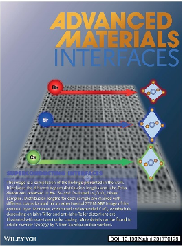
[2] Y. E. Suyolcu, Y. Wang, F. Baiutti, A. Al-Temimy, G. Gregori, G.Cristiani, W. Sigle, J. Maier, P. A. van Aken & G. Logvenov, “Dopant size effects on novel functionalities: High-temperature interfacial superconductivity”, Scientific Reports, 7 (2017), 453.
Research question that defines the REU student's project:
How precise can we control the structural quality of the epitaxial superconducting films?
Project plan/research task to answer the research question:
As a first step, the appropriate substrate and growth conditions will be chosen by the mentor and the student. The growth of the superconducting thin films will be monitored by in-situ RHEED, which will assist to confirm the absence of any additional undesired phases. We will then focus on ex-situ XRD measurements to examine the crystallinity and the structural quality of the samples. In parallel, x-ray reflectometry (XRR) measurements will also be conducted by the student under supervision of the mentor and the student will calculate the thickness of the grown films. The data analyses and related interpretation, including lattice parameter calculation and phase determination, will be employed by the student and will be discussed with the supervisor. After completing these characterization steps and confirming the high-quality, the samples will be ready for electrical transport measurements and future atomic-resolution STEM investigations.
List of tasks to be performed by the REU student and tasks to be performed by the mentor to answer the research questions:
- Epitaxial growth of high-temperature superconducting thin films. [To be conducted by the mentor, student to attend the experiments]
- In-situ control and characterization of thin films by RHEED during the growth. [To be conducted by the mentor, student to attend the experiments]
- Ex-situ control and characterization of thin films by XRD subsequent to the growth. [To be conducted by the student]
- XRD data plotting and analyses including lattice-parameter and film-thickness determination [To be conducted by the student]


