PARADIM Highlight #109—Local User Project (2025)
Darrell Schlom, Debdeep Jena, Grace Xing (Cornell), Zi-Kui Liu (Penn State), and Suman Datta (Notre Dame)
Transparent oxide thin film transistors (TFTs) are an important ingredient of transparent electronics. Their fabrication at the back-end-of-line (BEOL) opens the door to novel strategies to more closely integrate logic with memory for data-intensive computing architectures that overcome the scaling challenges of today's integrated circuits.
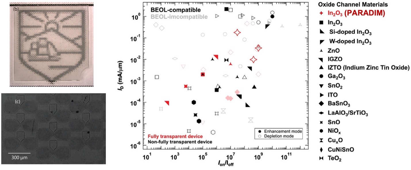
Figure 1: (Left, top) Brightfield micrograph of an epitaxial In2O3 10mm × 10mm sample grown by S-MBE with a transistor structure demonstrating the full transparency of the devices. (Left, bottom) Darkfield micrograph of the same sample at a higher magnification where the outline of the transistor structures can be seen. (Right) Comparison of the saturation drain current ID and the currents on/off ratio (Ion/Ioff) achieved for the devices shown in this work (red crosses) together with the best values from the literature. Devices fabricated at BEOL-incompatible temperatures are shaded. Fully-transparent devices are marked in red. Not fully transparent devices usually rely on a non-transparent contact. Solid symbols denote devices operated in enhancement mode, while devices operated in depletion mode are marked with open symbols.
Here, PARADIM users first apply a variant of molecular-beam epitaxy (MBE) called suboxide MBE (S-MBE) to grow epitaxial indium oxide (In2O3) at BEOL temperatures with unmatched crystal quality. They then use these high-quality indium oxide films as the channel layer in TFTs and demonstrate the highest performance fully transparent oxide TFTs ever reported. The key behind these results is the ability of S-MBE to navigate kinetic pathways. Providing a pre-oxidized molecular beam of In2O by S-MBE—instead of a beam of indium atoms as would be used in conventional MBE—bypasses the rate limiting step to the formation of In2O3 allowing it to be fabricated at low temperature with unprecedented structural and electronic perfection.
We have achieved the highest performance fully transparent oxide thin-film transistor (TFT). Not only does it outperform all prior fully transparent oxide TFTs, but it is made at the low temperatures used at the back end of the line of complementary metal-oxide-semiconductor (CMOS) semiconductor manufacturing.
TFTs are an important ingredient of transparent electronics. Their fabrication at the back-end-of-line (BEOL) opens the door to monolithic 3D integration of semiconductor channels to more closely integrate logic with memory for data-intensive computing architectures that overcome the scaling challenges of today’s integrated circuits by moving conventional planar semiconductor technology into the third dimension.
A variant of molecular-beam epitaxy (MBE) called suboxide MBE (S-MBE) that was developed (and patented [P. Vogt, D.G. Schlom, F.V.E. Hensling, K. Azizie, Z-K. Liu, B.J. Bocklund, and S-L. Shang, “Suboxide Molecular-Beam Epitaxy and Related Structures,” U.S. Patent #11,462,402 B2, granted October 4, 2022.]) by PARADIM users is demonstrated to be capable of growing epitaxial In2O3 at BEOL temperatures with unmatched crystal quality as evidenced by rocking curves, hybrid peaks and thickness oscillation in diffractograms, and STEM. The fullwidth at half maximum of the rocking curve is 0.015° and, thus, ≈5x narrower than any reports at any temperature to date and limited by the substrate quality. The key to achieving these results is the provision of an In2O beam by S-MBE, which enables growth in adsorption control and is kinetically favorable. Our results demonstrate the tremendous potential of In2O3 grown by S-MBE for TFTs.
It took PARADIM’s in-house research team working with a collaborator of the Platform 3 years to develop the comprehensive thermodynamic understanding underlying S-MBE. That itself is not unusual. What is unusual, at least from the traditional means of informing others through publication, is that PARADIM began openly sharing the concept of suboxide MBE and preliminary thermodynamic calculations with its users over 2 years prior to publication. This is part of the brainstorming that occurs among members of the Platform as they formulate plans to attempt to make new materials. This goes beyond just informing users of what has been done, but actively brainstorming as a team how to approach the synthesis of their specific systems of interest to realize what has never before been achieved. S-MBE has led to 22 journal publications by PARADIM’s community of practitioners to date, including this one. Further, it has been or is being used in 34 PARADIM projects. Note how quickly external users have become aware of the technique and have been able to apply it to the realization of materials of interest to them. This is a different way of doing business; it demonstrates the power of a MIP.
F.V.E. Hensling, P. Vogt, J. Park, S.-L. Shang, H. Ye, Y.-M. Wu, K. Smith, V. Show, K. Azizie, H. Paik, D. Jena, H.G. Xing, Y.E. Suyolcu, P.A. van Aken, S. Datta, Z.-K. Liu, and D.G. Schlom, "Fully Transparent Epitaxial Oxide Thin-Film Transistor Fabricated at Back-End-of-Line Temperature by Suboxide Molecular-Beam Epitaxy," Adv. Electron. Mater. 11, 2400499 (2025).
F.V.E.H., V.S., H.P., and D.G.S. acknowledge support from the National Science Foundation [Platform for the Accelerated Realization, Analysis, and Discovery of Interface Materials (PARADIM)] under Cooperative Agreement No. DMR-2039380. P.V., J.K., H.Y., K.S., D.J., H.G.X., S.D, and D.G.S. acknowledge the support from SUPREME and PRISM, two of seven centers in JUMP 2.0, a Semiconductor Research Corporation (SRC) program sponsored by DARPA. K.A. acknowledges the support from the AFOSR/AFRL ACCESS Center of Excellence under Award No. FA9550-18-1-0529. Substrate preparation was performed in part at the Cornell NanoScale Facility, a member of the National Nanotechnology Coordinated Infrastructure (NNCI), which is supported by the National Science Foundation (Grant No. NNCI-2025233). S.L.S. and Z.K.L. acknowledge support from the Endowed Dorothy Pate Enright Professorship at the Pennsylvania State University. This work made use of the Cornell Center for Materials Research Shared Facilities, which are supported through the NSF MRSEC program (DMR-1719875). F.V.E.H. acknowledges funding by the Alexander von Humboldt foundation in the form of a Feodor Lynen fellowship. The authors acknowledge Sean Palmer for substrate preparation and technical support. The authors thank Lena N. Majer for technical support and Marion Kelsch for TEM specimen preparation.