Introduction:
A cheap alternative to classical silicon solar cells is based on halide perovskites—a class of materials that can be easily deposited and processed in thin film form. The material matured from the laboratory to technological relevance within only ten years of intensive research. Currently, the efficiency of halide perovskite solar cells reaches the benchmark of state-of-the-art silicon solar cells.
Defects in the structure of a material, such as missing atoms or boundaries between grains oriented in different directions, may drastically inhibit the flow of electric currents through the material. The situation gets more complicated if a thin film of the material is needed and there are no large-area substrates that could act as suitable template to align all of the grains. For example, the depositing atoms may bond so strongly with the substrate that they cannot move around to make room for each other, or a weakly interacting substrate might not aid the alignment of the depositing atoms and they clump into grains that are misoriented from one another as well.
Jiang et al. study the growth and properties of thin films of CsPbBr3—a novel semiconductor material for solar cell applications. They find that lining a substrate that normally bonds too strongly with an atomically-thin layer of graphene weakens the bonding sufficiently for thin films to be grown with good alignment, larger grains, fewer defects, and significantly enhanced charge transport properties.
PARADIM provided access to high-resolution transmission electron microscopy to unravel the details of the interface between the substrate, graphene, and the thin film semiconductor.
J. Jiang et al. Nature Communications 10 (2019) 4145.
|
|
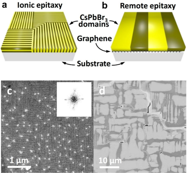
Figure: Schematic illustrations on remote epitaxy. The sketch a on the left illustrates ionic epitaxy, where a thin film is directly grown on the ionic substrate. Sketch b on the right shows the remote epitaxy, where a graphene layer is covering the entire substrate and the thin film is subsequently grown on the graphene. Scanning electron microscopy images of domain patterns are shown in c and d. For ionic epitaxy tiny domains are observed. In the right image for a sample of the same material grown via remote epitaxy the domains are much larger and exhibit less defects. |
Technical Information:
Halide perovskite has long been considered a “defect tolerant” material, where flaws in the crystallographic lattice like missing atoms or a mismatch known as dislocation are having less impact on the carrier dynamics compared to classical semiconductors. Although, first promising applications in optoelectronic devices have been demonstrated, the dislocation’s impact on the carrier dynamics of the material is largely unknown.
Jiang et al. investigate the relation between dislocation density and charge carrier dynamics in epitaxial halide perovskite films. First-principle calculations and molecular-dynamics simulations reveal that the dislocation density can be reduced if the film-substrate interaction is weakened. This is achieved via remote epitaxy, where a atomically thin layer, e.g. graphene, is introduced to cover the entire substrate and to act as a spacer between substrate and the epitaxial film. High-resolution transmission electron microscopy, Cs-corrected scanning transmission electron microscopy, and high-resolution atomic force microscopy are used to unveil the dislocation structure of the halide perovskite thin film. Growing the halide perovskite on various substrates (with and without the graphene cover) Jiang et al. were able to observe the negative impact of dislocations on the carrier dynamics. Reducing dislocation densities by more than one order of magnitude via remote epitaxy increases the electron lifetime by a factor of four. The study provides insights to develop free-standing films of halide perovskite, with low dislocation densities and improved charge carried dynamics.
The work was conducted at the Rensselear Polytechnic Institute’s Department of Materials Science and Engineering and the Department of Physics, Applied Physics and Astronomy, with contributions from Kunming University of Science and Technology, Tsinghua University, University of Science and Technology Beijing, Forschungszentrum Jülich, and Brown University.
Full reference: J. Jiang, X. Sun, X. Chen, B. Wang, Z. Chen, Y. Hu, Y. Guo, L. Zhang, Y. Ma, L. Gao, F. Zheng, L. Jin, M. Chen, Z. Ma, Y. Zhou, N.P. Padture, K. Beach, H. Terrones, Y. Shi, D. Gall, T.-M. Lu, E. Wertz, J. Feng and J. Shi, “Carrier lifetime enhancement in halide perovskite via remote epitaxy,” Nature Communications 10 (2019) 4145.