Materials discovery is more than calculating the properties that a material should have if the atoms were in desired positions. It is also key to get the atoms into those desired positions, to see what the properties really are, and thus realize the potential benefit of a new material. Making this happen takes a combination of ideas, capabilities, and execution—as the recent success by a team led by Assistant and Associate Professors from the University of Michigan illustrates.
 |
|
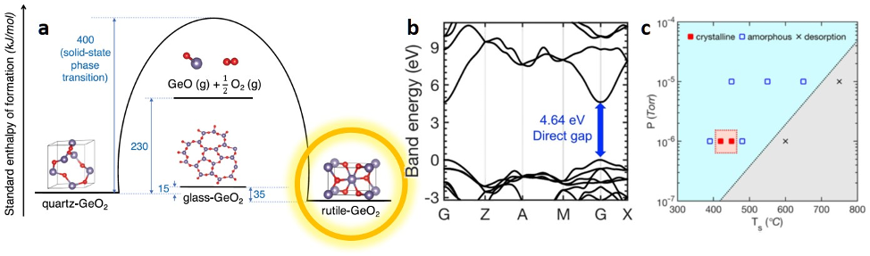
Figure 1: Rutile-GeO2, a promising material: identified by theory—realized at PARADIM. a) Reaction coordinate energy diagram for common phases of GeO2, including quartz GeO2, glass GeO2, and rutile GeO2, and the volatile species GeO. b) Band structure of rutile GeO2 with the direct bad gap of 4.64 eV indicated. c) Phase diagram of substrate temperature and ozone pressure used for the growth of various samples. Property of the achieved sample (crystalline or amorphous) is indicated. |
Theoretical work by the team established that rutile-GeO2—with its ultra-high band gap (4.64 eV), high mobility, high heat conductivity, and desired dopability—could provide superior performance for power electronics. But can this material be made as a thin film? The common synthesis approach would rely on deposition of the constituting elements, but for GeO2 growth is obstructed by a metastable glass phase and the volatile molecule GeO.
The team came to PARADIM and employed a recently established approach of “sub-oxide MBE”—using partially oxidized GeO instead of Ge—to realize the material in thin film form. Sieun Chae, the same graduate student who did the first-principles calculations, also grew the films. Her work has realized the first single crystal rutile-GeO2 thin films.
What Has Been Achieved:
Ultrawide bandgap (UWBG) semiconductors (Eg >3 eV) have tremendous potential for power-electronic applications. The current state-of-the-art UWBG materials such as β-Ga2O3, diamond, and AlN/AlGaN, however, show fundamental doping and thermal conductivity limitations that complicate technological adaption and motivate the search for alternative materials with superior properties. Rutile GeO2 (r-GeO2) has been theoretically established to have an ultrawide bandgap (4.64 eV), high electron mobility, high thermal conductivity (51 W m−1 K−1), and ambipolar dopability. While single-crystal r-GeO2 has been synthesized in bulk, the synthesis of r-GeO2 thin films has not been previously reported but is critical to enable microelectronics applications. Here, we report the growth of single-crystalline r-GeO2 thin films on commercially available R-plane sapphire substrates using molecular beam epitaxy. Due to a deeply metastable glass phase and high vapor pressure of GeO, the growth reaction involves the competition between absorption and desorption as well as rutile and amorphous formation. We control the competing reactions and stabilize the rutile-phase growth by utilizing (1) a buffer layer with reduced lattice misfit to reduce epitaxial strain and (2) the growth condition that allows the condensation of the preoxidized molecular precursor yet provides sufficient adatom mobility. The findings advance the synthesis of single-crystalline films of materials prone to glass formation and provide opportunities to realize promising ultra-wide-bandgap semiconductors.
Importance of the Achievement:
Demonstration of thin film growth of ultra-wide-bandgap semiconductor GeO2. Determination of first key properties
Unique Feature(s) of the MIP that Enabled this Achievement:
Molecular Beam Epitaxy at PARADIM’s Thin Film Facility using the recently established approach of “sub-oxide MBE”
The project was initiated by scientists from University of Michigan combining partners from theory and experiment, wherein PARADIM enabled the successful realization of the material.
Full Reference: S. Chae, H. Paik, N.M. Vu, E. Kioupakis, and J.T. Heron, “Epitaxial Stabilization of Rutile Germanium Oxide Thin Film by Molecular Beam Epitaxy,” Appl. Phys. Lett. 117, 072105 (2020). https://doi.org/10.1063/5.0018031
Data Availability: Raw data are available at https://data.paradim.org/194 provided by the PARADIM Data Collective.
Acknowledgement: We gratefully acknowledge Christopher Parzyck for SEM and EDXS measurements. Experimental work was supported by the National Science Foundation [Platform for the Accelerated Realization, Analysis, and Discovery of Interface Materials (PARADIM)] under Cooperative Agreement No. DMR-1539918. N.V. and J.H. acknowledge support from the Semiconductor Research Corporation (SRC) as the NEWLIMITS Center and NIST through the Award No. 70NANB17H041. H.P. acknowledges support from the National Science Foundation [Platform for the Accelerated Realization, Analysis, and Discovery of Interface Materials (PARADIM)] under Cooperative Agreement No. DMR-1539918. Substrate preparation was performed in part at the Cornell NanoScale Facility, a member of the National Nanotechnology Coordinated Infrastructure (NNCI), which is supported by the NSF (Grant No. NNCI-1542081).