One Materials-by-design commonly starts with first principles theory to identify materials with desired properties. The significant energetic contribution of electron-electron interactions, however, makes it difficult for theory to accurately predict quantum materials. Experimental tools like ARPES that measure electronic band structure directly used in combination with synthesis tools like MBE make it possible to enter the materials-by-design loop from a different on-ramp and navigate quantum materials to achieve desired properties.
 |
|
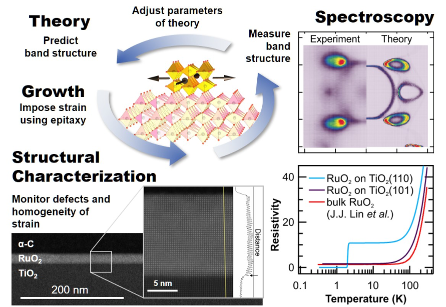
Figure 1: a) The Materials-by-Design loop combines the theoretical prediction of a material with desired properties, the realization by MBE, its structural characterization by STEM, and spectroscopy to verify the achieved electronic properties. b) Structural characterization by STEM is used to monitor defects and the homogeneity of the strain. c) Spectroscopy, including ARPES, is used to verify the achieved electronic properties and to inform how adjustments of theoretical parameters might enhance the predictive power. |
Using epitaxial strain, PARADIM’s in-house research team transmuted a metal into a superconductor for the first time. With their unique tools, PARADIM scientists were able to apply strain in different directions to a thin film of RuO2 and using ARPES follow its effect on the band structure. The RuO2 remained metallic, but a band with a high density of states could be moved close to the Fermi level. When this occurred, the RuO2 became superconducting. The ability to deterministically enhance the superconducting transition temperature by design, rather than by serendipity, has been a long sought-after goal in condensed matter physics and materials science. PARADIM’s approach can be expanded to various related quantum materials, particularly other oxide quantum materials.
What Has Been Achieved: PARADIM’s in-house research team reports the discovery of superconductivity in thin films of a material (RuO2) previously not known to be superconducting. We employ a combination of electrical transport, x-ray diffraction, and angle-resolved photoemission spectroscopy (ARPES) measurements to demonstrate that the superconductivity is caused by epitaxial strains imposed on the RuO2 thin films by the isostructural TiO2 substrates upon which they are grown. By comparing strain-induced changes to the electronic structure as measured by ARPES with the predictions of density functional calculations, we show that appropriately chosen anisotropic strains in this multi-orbital system depopulate at bands with djj orbital character away from being completely filled, which substantially increases the density of states near the Fermi level and likely contributes to the marked enhancement of superconductivity observed in strained RuO2.
Importance of the Achievement: Strain-stabilized RuO2/TiO2(110) is the first known stoichiometric superconductor within the rutile family, demonstrating a promising strategy to create new transition-metal superconductors based on judiciously chosen anisotropic strains.
Unique Feature(s) of the MIP that Enabled this Achievement: Realizing this challenging approach was made possible by PARADIM’s In-House Research Team and PARADIM Theory and Simulation staff pulling together to collaboratively identify a synthesis path and making use of a signature tool that combines MBE, ARPES, XPS, LEED, R vs. T with input from STEM and electronic property calculations.
Publication: J.P. Ruf, H. Paik, N.J. Schreiber, H. P. Nair, L. Miao, J.K. Kawasaki, J.N. Nelson, B.D. Faeth, Y. Lee, B.H. Goodge, B. Pamuk, C.J. Fennie, L.F. Kourkoutis, D.G. Schlom, and K.M. Shen, “Strain-Stabilized Superconductivity,” Nat. Commun. 12, 59 (2021) DOI: 10.1038/s41467-020-20252-7.
Data Availability:Data is available through the PARADIM Data Collective at http://data.paradim.org/169/ and with a citable DOI: https://doi.org/10.34863/b0f9-f889.
Acknowledgement:The authors thank Y. Li for assistance with electrical transport measurements. This work was supported through the National Science Foundation (Platform for the Accelerated Realization, Analysis, and Discovery of Interface Materials, PARADIM) under Cooperative Agreement No. DMR-1539918, NSF DMR-1709255, the Air Force Office of Scientific Research Grant No. FA9550-15-1-0474, and the Department of Energy (Award No. DE-SC0019414). This research was funded in part by the Gordon and Betty Moore Foundation’s EPiQS Initiative through Grant No. GBMF3850 to Cornell University. This work made use of the Cornell Center for Materials Research (CCMR) Shared Facilities, which are supported through the NSF MRSEC Program (No. DMR-1719875). The FEI Titan Themis 300 was acquired through NSF-MRI-1429155, with additional support from Cornell University, the Weill Institute, and the Kavli Institute at Cornell. Device fabrication and substrate preparation were performed in part at the Cornell NanoScale Facility, a member of the National Nanotechnology Coordinated Infrastructure (NNCI), which is supported by the NSF (Grant No. ECCS-1542081).