Building on their growing expertise with valleytronic materials, PARADIM researchers, Jiwoong Park (University of Chicago) and David Muller (Cornell University) have discovered a way to assemble multi-layer stacks of monolayers of transition metal dichalcogenide (TMD) materials (MoS2, MoSe2, and WS2) with centimeter-scale dimensions in a user-defined sequence. The assembly is achieved without the use of etchants or solvents by exploiting the stronger binding that occurs between TMD layers than between the TMD layer and the underlying substrate.
|
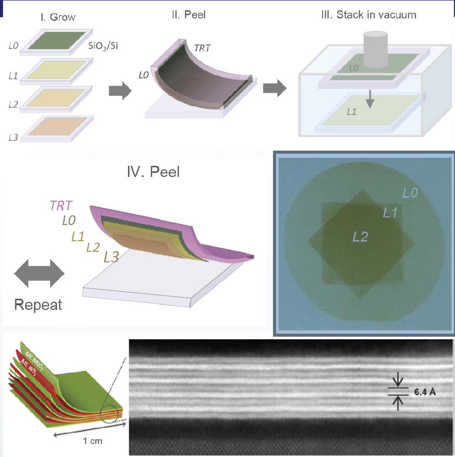
| Figure 1: Procedure of Program Vacuum Step Process with TMD sample and resulting layers imaged with light microscopy and TEM. |
Superlattices, bandgap engineered tunnel diodes, and tunnel device arrays with nearly ideal electrical properties have been demonstrated. Despite their large lateral extent, these made-to-order stacked structures show electrical properties that are not dominated by structural inhomogeneities that would strongly affect the tunnel current (e.g., cracks, wrinkles, or trapped impurities). This method enables TMDs to be combined in ways that are free of the constraints of lattice match or crystallographic alignment, enabling the layer-by-layer assembly of TMD-based device structures.
Reference: K.Kang et al., Nature 550(2017) 229–233.
Technical details:
High-performance semiconductor films with vertical compositions that are designed to atomic-scale precision provide the foundation for modern integrated circuitry and novel materials discovery. One approach to realizing such films is sequential layer-by-layer assembly, whereby atomically thin two-dimensional building blocks are vertically stacked, and held together by van der Waals interactions. With this approach, graphene and transition-metal dichalcogenides—which represent one- and three-atom-thick two-dimensional building blocks, respectively—have been used to realize previously inaccessible heterostructures with interesting physical properties. No large-scale assembly method exists, however, at present that maintains the intrinsic properties of these two-dimensional building blocks while producing pristine interlayer interfaces, thus limiting the layer-by-layer assembly method to small-scale proof-of-concept demonstrations.
PARADIM scientists report the generation of wafer-scale semiconductor films with a very high level of spatial uniformity and pristine interfaces. The vertical composition and properties of these films are designed at the atomic scale using layer-by-layer assembly of two-dimensional building blocks under vacuum. We fabricate several large-scale, high-quality heterostructure films and devices, including superlattice films with vertical compositions designed layer-by-layer, batch-fabricated tunnel device arrays with resistances that can be tuned over four orders of magnitude, band-engineered heterostructure tunnel diodes, and millimeter-scale ultrathin membranes and windows. The stacked films are detachable, suspendible and compatible with water or plastic surfaces, which will enable their integration with advanced optical and mechanical systems.
Full Reference: Kang, K., Lee, K., Han, Y. et al. Layer-by-layer assembly of two-dimensional materials into wafer-scale heterostructures. Nature 550, 229–233 (2017). https://doi.org/10.1038/nature23905
Return to: In-house Research Highlights