PARADIM Highlight #41—External User Project (2021)
Joshua Goldberger, W. Windl, and J.P. Heremans (Ohio State University) and D. Cahill (University of Illinois Urbana-Champaign)
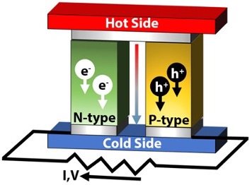
Figure 1: Schematic of a classical thermoelectric module of a pair of n- and p-type semiconductors between the hot and cold side
The direct conversion between heat and electricity that allows for active cooling or the use of waste heat for power generation is enabled by thermoelectric devices.
Traditional thermoelectric modules utilize hundreds of pairs of p-type and n-type semiconductors, where heat flows from top to bottom and the electric current meanders through the whole structure (see Figure 1). The sheer number of metal-semiconductor contacts causes large efficiency losses compared to the thermoelectric efficiency of the bare semiconductor. Also, the need for stable contacts at the hot side limits operating temperatures and device lifetimes.
In “transverse” thermoelectric devices—developed at Ohio State with the discovery of goniopolarity —a voltage develops perpendicular to the temperature gradient, requiring only one active material and no contacts near the hot side, avoiding a major source of energy loss and device degradation.
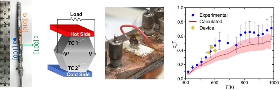
Figure 2 (from left): Rhenium silicide crystal grown at PARADIM; schematic of the transverse thermoelectric module; photograph of actual module; diagram of the temperature dependence of the thermoelectric efficiency, comparing theoretical prediction (red curve) and the experimental values (data points: blue dots and yellow stars).
The group came to PARADIM’s bulk crystal facility to grow sufficiently large single crystals of rhenium silicide (Re4Si7), a material with record transverse thermoelectric efficiency (see Figure 2). Constructing a transverse thermoelectric generator from a single crystal, the group confirmed that the device efficiency (yellow stars) shows no losses compared to the bare material (blue dots) and the calculated efficiency (red curve). The present work establishes transverse thermoelectrics as a viable technology, and rhenium silicide as the “gold-standard” transverse thermoelectric.
The principal challenges in current thermoelectric power generation modules are the availability of stable, diffusion-resistant, lossless electrical and thermal metal-semiconductor contacts that do not degrade at the hot end nor cause reductions in device efficiency. Transverse thermoelectric devices, in which a voltage develops in a direction perpendicular to the thermal gradient in a single material, promise to overcome these problems. However, the measured material transverse thermoelectric efficiencies, zxyT, of nearly all materials to date has been far too low to confirm these advantages in an actual device. Here, we show that single crystals of Re4Si7, an air-stable, thermally robust, layered compound, have a transverse zxyT of 0.7±0.15 at 980 K, a value that is on par with existing commercial longitudinal thermoelectrics today. Through constructing and characterizing a transverse power generation module, we prove that extrinsic losses through contact resistances are minimized in this geometry, and that no electrical contacts are needed at the hot side. This excellent transverse thermoelectric performance arises from the large, oppositely signed in-plane p-type and cross-plane n-type thermopowers. These large anisotropic thermopowers arise from thermal population of the highly anisotropic valence band and isotropic conduction band in this narrow gap semiconductor. Overall, this work establishes Re4Si7 as the “gold-standard” of transverse thermoelectrics, allowing future exploration of unique device architectures for waste heat recovery.
Importance of Achievement: Demonstration of a transverse thermoelectric device based on a single material confirming that the dominant source of energy loss in conventional thermoelectrics—the contacts—can be greatly reduced. Further, in this new class of thermoelectrics all electric contacts can be placed away from the hot side to avoid a major source of device degradation. This opens the door to new families of thermoelectric materials that will lead to improve energy capture and efficiency across a range of applications.
Figure 3: NSF Science Nation, Episode 332: "Quantum Crystals - Creating new Families of Electronic Materials"
This work was enabled by the floating zone suite within the Bulk Crystal Growth facility, which enabled growth of Re4Si7 across size scales in the tilting laser diode and xenon optical floating zone furnaces.
The work has been featured in
- NSF Science Nation, Episode 332: “Quantum Crystals – Creating new Families of Electronic Materials” https://www.nsf.gov/news/mmg/mmg_disp.jsp?med_id=187313
- Phys.org https://phys.org/news/2021-05-gold-standard-compound-electricity.html
- Science Times https://www.sciencetimes.com/articles/31399/20210527/new-layered-crystal-steps-up-future-thermoelectric-devices.htm
- Ohio State News https://news.osu.edu/a-new-gold-standard-compound-for-generating-electricity-from-heat
- Electronics Weekly https://www.electronicsweekly.com/news/research-news/silicon-rhenium-make-transverse-electricity-heat-2021-05/
M.R. Scudder, B. He, Y. Wang, A. Rai, D. Cahill, W. Windl, J.P. Heremans, and J. Goldberger, "Highly Efficient Transverse Thermoelectric Devices with Re4Si7 crystals,” Energy Environ. Sci. 14, 4009-4017 (2021).
Primary funding this work synthesis, theory, and transport measurements (M.R.S., J.E.G., Y.W., and W.W.) was provided by AFOSR project no. FA9550-18-1-0335 and DOE grant number DE-SC0020923 (J.P.H.). Funding for thermal conductivity measurements (A.R., D.G.C.) and transport measurements (B.H.) was provided by NSF EFRI-1433467. This material is based upon single crystal growth supported by the: National Science Foundation (Platform for the Accelerated Realization, Analysis, and Discovery of Interface Materials (PARADIM)) under Cooperative Agreement No. DMR-1539918. Computations were performed on the machines of the Ohio Supercomputer Center under project no. PAS0072.
Data detailing the growth of Re4Si7 single crystals are publicly available at https://data.paradim.org/122.