PARADIM Highlight #42—In-House Research (2021)
Electron microscopy is a widespread and often essential tool for structural and chemical analysis at the atomic level. Image resolution is dominated by the energy (or wavelength) of the electron beam and the quality of the lens. By combining our new design of electron microscope pixel array detector (EMPAD), which has the dynamic range to record the complete distribution of transmitted electrons at every beam position and a phase retrieval algorithm to process the data, PARADIM’s in-house research team has increased the spatial resolution well beyond the traditional lens limitations, setting a world record in 2018 for the highest resolution microscope (0.39 Å Abbe resolution [1]) at the same dose and imaging conditions where conventional imaging modes reach only 0.98 Å. The EMPAD is the culmination of over a decade of detector development at Cornell, supported by NSF (through CHESS, CCMR), DOE, the WM Keck Foundation, and the Kavli Institute, and has been commercially licensed by ThermoFisher Scientific and is now manufactured and sold at scale.
Our next-generation EMPAD prototype, with an order of magnitude increase in speed and data rate, has made it possible to image thicker samples at double the spatial resolution (<0.20 Å Abbe resolution), limited mainly by the random thermal motions of the atoms themselves. This new super-resolution imaging is available to PARADIM users utilizing the new EMPAD detector in combination with multislice ptychography in (and only in) PARADIM’s electron microscopy user facility.
It has long been recognized that the information limit set by diffractive optics is not an ultimate limit. Instead, there is phase information encoded throughout a diffraction pattern formed from a localized electron beam. It is in the form of interference patterns between overlapping scattered beams, and as the incident localized beam is scanned, the phase information and hence the interference patterns change in a predictable manner that can be used to retrieve the phase differences, an approach known as ptychography. While originally conceived to solve the phase problem in crystallography, ptychography has received renewed attention as a dose-efficient technique to recover the projected potential of materials, with modifications to measure finite thickness and three-dimensional samples. In principle the resolution is limited by the largest scattering angle at which meaningful information can still be recorded, however, as electron scattering form factors have a very strong angular dependence, the signal falls rapidly with scattering angle, requiring a detector with high dynamic range and sensitivity to exploit this information.
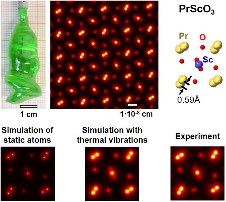
To date, ptychography has been widely adopted for light and x-ray applications, yet the technique is still under-explored in transmission electron microscopy in large part because of the detector challenges. Traditional electron cameras such as charge-coupled devices (CCDs) and pixelated detectors have been hampered by slow readout speeds or poor dynamic ranges. Previous work has mainly made use of electrons only within the bright field disk and thus image resolution did not overcome the 2α limit imposed by the physical aperture. Based on decades of experience of detector development at CHESS, we developed and employ a new type of electron microscope pixel array detector (EMPAD) that is capable of recording all the transmitted electrons with sufficient sensitivity and speed to provide a complete ptychographic reconstruction—recognized as the highest resolution microscope (of any type) by Guinness World Records in July 2018. Our EMPAD design has a high dynamic range of 1,000,000:1 while preserving single electron sensitivity with a signal-to-noise ratio of 140 for a single electron at 200 keV. The detector retains a good performance from 20-300 keV. Here we operated at 300 keV and a maximum beam current of 33 pA. By utilizing essentially all collected electrons (99.95% of the incident beam), with a full 4D data set acquired in typically a minute, our full-field ptychographic reconstructions more than doubles the image resolution compared to the highest-resolution conventional imaging modes such as annular dark field STEM.
The new 0.2 Å resolution images were measured in 300-Å-thick PrScO3, and the multiple scattering was corrected using a multislice ptychography algorithm. The spatial resolution is now largely limited by the thermal fluctuations of the atoms themselves.
PARADIM in-house researchers developed the EMPAD detector, refined the ptychography algorithm to analyze the data, and implemented a multislice approach to allow for the investigation of nm-thick samples. Methods are made available for all users of PARADIM.
- Popular Science https://www.popsci.com/science/highest-microscope-resolution-individual-atoms/
- Cornell Chronicle https://news.cornell.edu/stories/2021/05/cornell-researchers-see-atoms-record-resolution
- Scientific American https://www.scientificamerican.com/article/see-the-highest-resolution-atomic-image-ever-captured/
Z. Chen, Y. Jiang, Y. Shao, M.E. Holtz, M. Odstrčil, M. Guizar-Sicairos, D.G. Schlom, and D.A. Muller. “Electron ptychography achieves atomic-resolution limits set by lattice vibrations,” Science 372 (2021) 826-831, DOI: 10.1126/science.abg2533
D.A.M. thanks M. Humphry of Phasefocus for helpful discussions on multislice 3D ptychography. Funding: This research was supported by the National Science Foundation under grant DMR-1539918 (PARADIM Materials Innovation Platform in-house program). Electron microscopy performed at the Cornell Center for Materials Research was supported by the National Science Foundation under grant DMR-1719875.
Additional Material: Access to data and software codes is provided through the PARADIM Data Collective at data.paradim.org and the corresponding DOIs 10.34863/ssmm-2j11 and 10.5281/zenodo.4659690.
Funding sources:
- Detector development (both early x-ray versions and electron version since 2006) – NSF (CHESS, the CCMR MRSEC, MIP-PARADIM), DOE BES, the WM Keck Foundation, and the Kavli Institute;
- Ptychography – MIP-PARADIM
The detector has been licensed to Thermo Fisher Scientific and is now manufactured and sold commercially at scale.
References:
- Y. Jiang, Z. Chen, Y. Han, P. Deb, H. Gao, S. Xie, P. Purohit, M. W. Tate, J. Park, S. M. Gruner, V. Elser, and D. A. Muller. “Electron Ptychography of 2D Materials to Deep Sub-Ångström Resolution,” Nature 559, 343–349 (2018).
- Z. Chen, M. Odstrcil, Y. Jiang, Y. Han, M.-H. Chiu, L.-J. Li, and D.A. Muller, “Mixed-state electron ptychography enables sub-angstrom resolution imaging with picometer precision at low dose,” Nat. Commun. 11, 2994 (2020).