PARADIM Highlight #44—External User Project (2021)
Jian Shi (Rensselaer Polytechnic Institute)
Many electronic devices, like non-volatile high-density memories, ultra-fast switches, and thin film capacitors, rely on ferroelectric materials—a class of materials with spontaneous electrical polarization which can be reproducibly switched. In two-dimensional (2D) and quasi-2D ferroelectric materials the size of ferroelectric domains can be small which may enable the miniaturization of devices. Understanding of ferroelectric domain structure at the atomic scale is, however, limited, hindering the development of functional device units at the microscopic level.
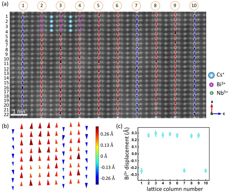
Figure 1: Unit-cell-thick ferroelectric domains with 180° domain walls. (a) Scanning transmission electron microscopy (STEM) image of free-standing CsBiNb2O7. The theoretical lattice structure of CBNO is overlaid onto the atomic image. Blue and red arrows indicate the relative displacement of a Bi3+ ion with respect to the center of its two neighboring Cs+ ions. (b) The top 8 rows of arrows in (a) without the STEM image for clarity. The magnitudes of the Bi3+ displacement vectors are represented by the arrow area and color. (c) Displacements of Bi3+ along the a axis relative to the center of two neighboring Cs+ ions are averaged over each indexed column in (a) and are plotted vs the lattice column number. Error bars represent standard deviation.
Here, CBNO (cesium bismuth niobate CsBiNb2O7)—a layered oxide that has been predicted to be ferroelectric with a high Curie temperature and large in-plane polarization—is employed as a model system to study its ferroelectric domain structure at the atomic scale in PARADIM’s electron microscopy user facility. By aberration-corrected scanning transmission electron microscopy, which allows precise tracking of atomic positions, the user from RPI revealed the existence of ferroelectric domains that are just one unit-cell-thick and 180° domain walls with an abrupt change in polarization direction in free-standing CBNO. The work might inspire new design concepts for ferroelectric devices demanding unit-cell-thick domain structures.
Two-dimensional (2D) and quasi-2D ferroelectric materials have demonstrated their potential for enabling device miniaturization. The fundamental understanding of the ferroelectric domain structure at atomic scale is limited, however, hindering development of functional device units at the microscopic level. In this paper, we employ a Dion–Jacobson layered oxide CsBiNb2O7 (CBNO), which has been predicted to be ferroelectric with high Curie temperature and large in-plane polarization, as a model system to study its ferroelectric domain structure with atomic scale analysis. We reveal the existence of unit-cell-thick ferroelectric domain size as well as both 180° and 90° domain walls in free-standing CBNO. In an epitaxial CBNO film grown on a LaAlO3 substrate, we discover multiple stacking structures resembling the Aurivillius and the Ruddlesden–Popper phases. We also analyze the interfacial dislocations and their associated lattice distortion fields in the epitaxial film. This paper may inspire design concepts for ferroelectric devices demanding unit-cell-thick domain size.
Importance of Achievement: This paper demonstrates exceptionally narrow ferroelectric domains and domain walls in a quasi-2D oxide which may inspire new design concepts for next-generation microelectronic devices, such as nonvolatile high-density memories and synaptic devices.
The work made use of PARADIM’s electron microscopy suite for both preparation of high-quality cross-sections of free-standing CBNO and for mapping the atomic-scale ferroelectric domain structure by aberration-corrected scanning transmission electron microscopy (STEM). Close collaboration between PARADIM users and staff enabled quantification of atomic positions and lead to the discovery of one unit-cell-thick ferroelectric domains in this material.
- Y. Guo, B.H. Goodge, L. Zhang, J. Jiang, Y. Chen, L.F. Kourkoutis, and J. Shi, "Unit-Cell-Thick Domain in Free-Standing Quasi-Two-Dimensional Ferroelectric Material," Phys. Rev. Materials 5, 044403 (2021). DOI: 10.1103/PhysRevMaterials.5.044403
- L. Zhang, J. Jiang, Y. Cai, S. Yao, B. Azhar, Z. Chen, Y. Hu, S. Pendse, Y. Guo, R. Jia, Z. Tian, C. Sun, P. Liao, and J. Shi, "Doping-Enabled Reconfigurable Strongly Correlated Phase in a Quasi-2D Perovskite," J. Phys. Chem. Lett. 12, 5091−5098 (2021). DOI: 10.1021/acs.jpclett.1c00353
Y.G. and J.S. acknowledge the Air Force Office of Scientific Research under Award No. FA9550-18-1-0116. L.Z. and J.S. acknowledge the NYSTAR Focus Center under Award No. C150117. This paper is supported by the National Science Foundation [Platform for the Accelerated Realization, Analysis, and Discovery of Interface Materials (PARADIM)] under Cooperative Agreement No. DMR-1539918 and made use of the Cornell Center for Materials Research (CCMR) Shared Facilities, which are supported through the NSF MRSEC Program (No. DMR-1719875). The FEI Titan Themis 300 was acquired through No. NSF-MRI-1429155, with additional support from Cornell University, the Weill Institute, and the Kavli Institute at Cornell. This paper is also partially supported by the National Science Foundation under Awards No. 2024972, No. 2031692, and No. 1916652.