PARADIM Highlight #53—Local User Project (2021)
B. Pamuk, D.A. Muller (PARADIM), with G. Khalsa, G.H. Xing, D. Jena (Cornell U.), and V. Strocov (PSI, Switzerland)
Currently, electronic device technology is based mainly on semiconductors. It first emerged in the middle of the 20th century and has improved ever since. Further technological advances including energy efficiency and information security might profit from exploiting quantum mechanical properties that are present in superconductors. The challenge is how to combine the two states and to make sure to get the best of both electrical worlds. A collaboration of researchers from Cornell and the Paul Scherrer Institute (PSI) in Switzerland grew thin films of the superconductor niobium nitride (NbN) on top of gallium nitride (GaN), a semiconductor and vital component in many optical and power electronics. The team measured the electronic properties of the two materials directly at their interface using soft-X-ray angle-resolved photoelectron spectroscopy (ARPES).
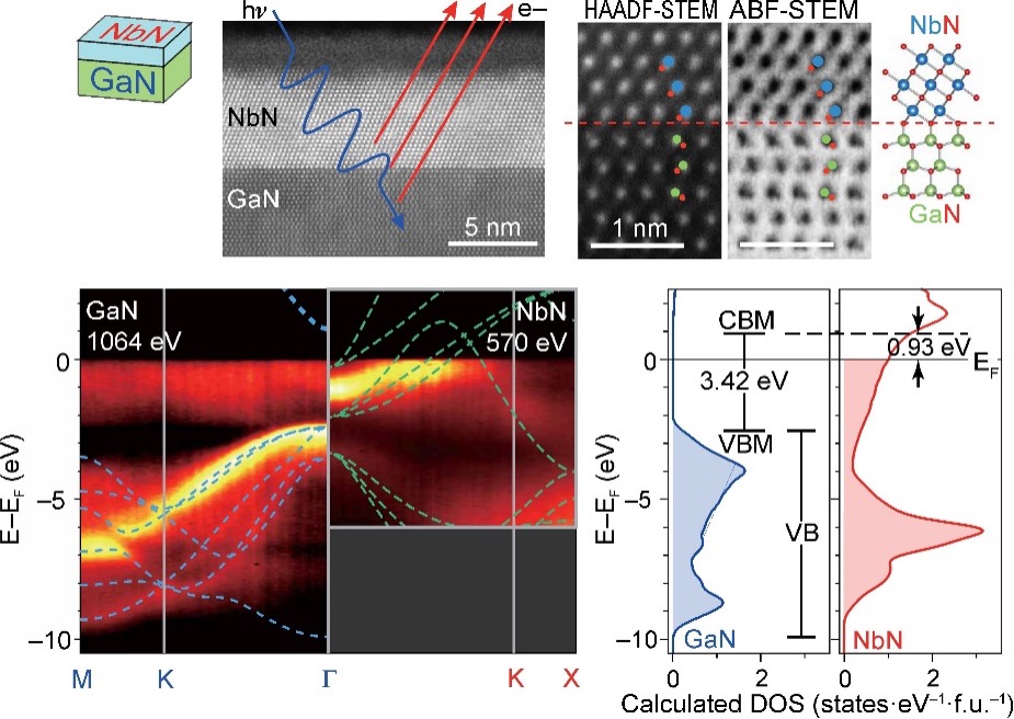
Figure 1: (top) Schematic of sample, high resolution transmission electron microscopy images of the interface with atomic structure overlaid. (bottom) Angle-resolved photoelectron spectroscopy at the interface with theoretical band structure of the two materials (dashed lines). Density of electronic states in bulk GaN and NbN calculated using density functional theory.
PARADIM's electron microscopy and theory user facilities provided structural characterization and first-principles calculations of the two materials and the superconductor-semiconductor interface. The electronic states of NbN and GaN at the Fermi level remain separated, therefore revealing that the superconducting property of NbN is unchanged when interfaced with GaN. The new momentum-resolved understanding of the electronic properties right at the interfaces opens up new frontiers for quantum materials where subtle effects at the interfacial states play a defining role.
Electronic structure at a heterointerface is the key to controlling the functionality of a device. Using soft x-ray angle-resolved photoelectron spectroscopy (SX-ARPES), the electronic structure of both sides of the Schottky heterointerface formed by epitaxial films of superconducting NbN on semiconducting GaN is measured in agreement with the electronic structure calculations from first principles conducted at PARADIM’s theory facility. We find that the electronic states at the Fermi level in NbN are separated in energy and momentum from the states in GaN, therefore revealing that the superconducting properties of NbN is unchanged when interfaced with GaN. The Schottky barrier height obtained from photoemission is corroborated by electronic transport and optical measurements. The momentum-resolved understanding of electronic properties of interfaces elucidated in our work opens up new frontiers for the quantum materials where interfacial states play a defining role.
Addressing design of future quantum devices, this study uncovers electronic structure of a superconductor-semiconductor interface. Understanding the electronic structure of the interface is critical in deterministically modifying the devices for our needs. In addition, this is the first direct measurement of the electronic structure of a nearly a century old superconductor NbN. The similarities and differences between the SX-ARPES measurement and the first-principles calculation of the band structure of NbN hints at further exploration of the electronic interactions needed to better understand its superconductivity.
The staff scientist of the theory user facility at PARADIM is a co-PI of the proposal about understanding and modifying the superconducting properties of transition-metal nitrides. All first-principles calculations are performed at PARADIM computational resources.
- PSI Newsroom: “Semiconductors Reach the Quantum World” https://www.psi.ch/en/media/our-research/semiconductors-reach-the-quantum-world
- Cornell Chronicle: “Collaboration Gets Quantum View Superconductor Junction” https://news.cornell.edu/stories/2021/12/collaboration-gets-quantum-view-superconductor-junction
T. Yu*, J. Wright*, G. Khalsa, B. Pamuk, C.S. Chang, Y. Matveyev, X. Wang, T. Schmitt, D. Feng, D.A. Muller, G.H. Xing, D. Jena, and V. Strocov, "Momentum-Resolved Electronic Structure and Band Offsets in an Epitaxial NbN/GaN Superconductor/Semiconductor Heterojunction," Sci. Adv. 7, abi5833 (2021), DOI: https://doi.org/10.1126/sciadv.abi5833.
The work at Cornell University was supported, in part, by the Office of Naval Research under grant no. N00014-17-1-2414 monitored by P. Maki, the National Science Foundation (NSF) under grant no. NewLAW EFMA 1741694, an AFOSR (grant no. FA9550-20-1-0048) award monitored by K. Goretta, NSF award no. DMREF-1534303, NSF RAISE-TAQS award no. 1839196, and the Cornell Center for Materials Research with funding from NSF MRSEC Program no. DMR-1719875. This work was performed, in part, at the Cornell NanoScale Science and Technology Facility (CNF), a member of the National Nanotechnology Coordinated Infrastructure (NNCI), which is supported by the NSF (grant no. NNCI-1542081). G.K. and B.P. acknowledge the NSF [Platform for the Accelerated Realization, Analysis, and Discovery of Interface Materials (PARADIM)] under Cooperative agreement no. DMR-1539918. T.Y. and D.F. acknowledge the National Natural Science Foundation of China (grant nos. 11790312, 11888101, and 12074074).
Data Availability:
Data associated with this project are available through the PARADIM Data Collective at DOI: https://doi.org/10.34863/b8x7-5y76/