PARADIM Highlight #58—In-House Research (2022)
Jiwoong Park (University of Chicago) and David A. Muller (Cornell University)
Quantum fabrics offer novel electronic, magnetic, or topological textures with functionalities that do not exist in bulk and could play an important role in future quantum technologies. Quantum fabrics are created by weaving together "threads" with different properties, such as superconductivity or magnetism. One method to make them is the atomically precise assembly of layered two-dimensional Van der Waals (vdW) materials. This assembly has traditionally been accomplished using artisan methods from micromechanical exfoliated flakes, but such fabrication is not compatible with scalable and rapid manufacturing.
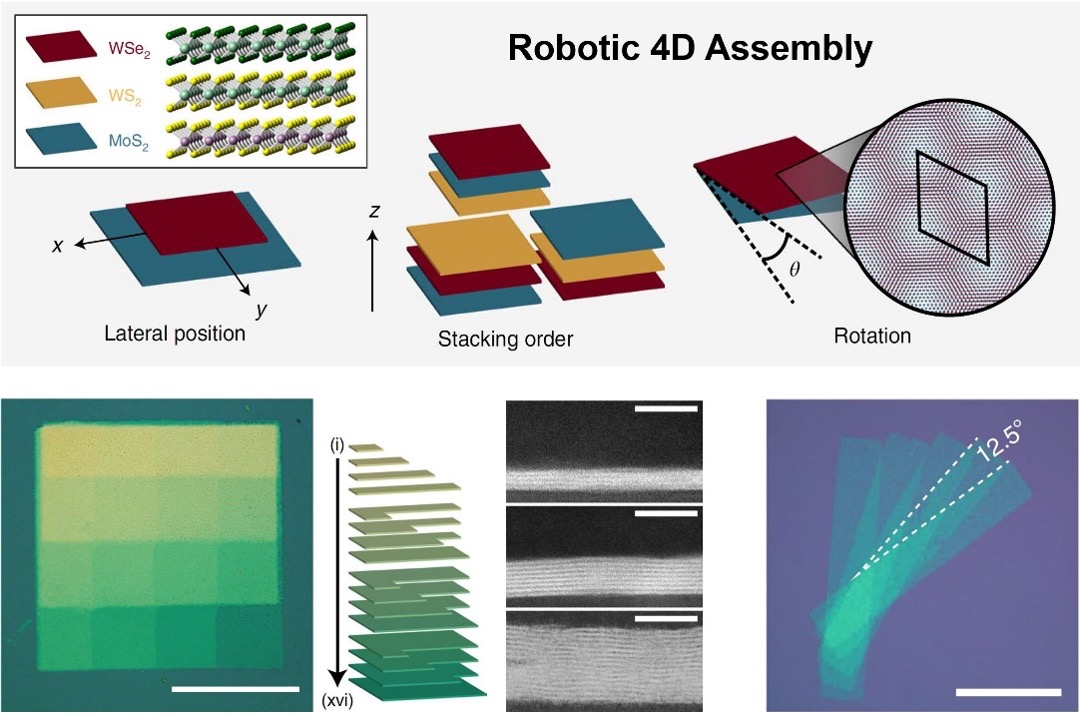
Figure 1: (top) Schematic of the four-dimensional assembly concept on stacking various two-dimensional materials. (bottom, left) Optical microscopy image of a 1-to-16 layer MoS2 grid structure (Scale bar 50 μm) and schematic of the 16 layers (i)–(xvi) to realize the 16-tile grid structure. (bottom, center) Cross-sectional STEM images of 4 L (top) , 8 L (middle) and 16 L (bottom) MoS2 extracted from the 1-16 grid, demonstrating atomically resolved thickness control (scale bars 10 nm). (bottom, right) Optical microscopy image of a robot-manufactured vdW solid demonstrating interlayer twist angle control (scale bars 50 μm).
Here, PARADIM’s In-House Research group demonstrates a robotic assembly method for creating stacks of vdW layers with unprecedented speed, deliberate design, angle control, and large area. The building blocks are prepatterned “pixels” made from atomically thin two-dimensional components, like monolayers of transition metal dichalcogenide (TMD) materials (MoS2, MoSe2, and WS2). The clean, contact-free process from growth, patterning to assembly in vacuum is used to fabricate vdW solids containing up to 80 individual layers consisting of 100x100μm2 areas with predesigned shapes, programmed composition and controlled interlayer angle. The PARADIM-developed method enables the rapid prototyping of quantum fabrics, which could help realize the full potential of vdW heterostructures as a platform for novel physics and advanced electronic technologies.
Van der Waals solids can be engineered with atomically precise vertical composition through the assembly of layered two-dimensional materials. However, the artisanal assembly of structures from micromechanically exfoliated flakes is not compatible with scalable and rapid manufacturing. Further engineering of vdW solids requires precisely designed and controlled composition over all three spatial dimensions and interlayer rotation. Here, PARADIM researchers report a robotic four-dimensional pixel assembly method for manufacturing vdW solids with unprecedented speed, deliberate design, large area and angle control—robotic assembly of prepatterned ‘pixels’ made from atomically thin two-dimensional components. Wafer-scale two-dimensional material films were grown, patterned through a clean, contact-free process and assembled using engineered adhesive stamps actuated by a high-vacuum robot. vdW solids with up to 80 individual layers, consisting of 100 × 100 μm2 areas with predesigned patterned shapes, laterally/vertically programmed composition and controlled interlayer angle are demonstrated. This enabled efficient optical spectroscopic assays of the vdW solids, revealing new excitonic and absorbance layer dependencies in MoS2. Furthermore, twisted N-layer assemblies enabled the observation of atomic reconstruction of twisted four-layer WS2 at high interlayer twist angles of ≥4°. The PARADIM-developed method enables the rapid prototyping of atomically resolved quantum materials, which could help realize the full potential of vdW heterostructures as a platform for novel physics and advanced electronic technologies.
Robotic 4D pixel assembly presents a new method for manufacturing precise vdW solids, highlighted by our two demonstrations of a one-shot optical assay and twisted multilayer stacking. Contrasting with existing fabrication methods based on exfoliated materials (where each device is unique), the presented manufacturing process could enable the efficient assembly of identical structures on the same chip. When combined with the growth of large single crystals of two-dimensional materials, the assembly technique could enable high-throughput investigation of engineered electronic states in more complex, multilayer twisted heterostructures. This also establishes an avenue for harnessing twisted structures in technological applications. Moreover, beyond wafer-scale synthesized TMDs, the processes of large-area material synthesis, precise patterning and automated assembly should generalize to other categories of materials that may be delaminated, such as thin-film electrodes, two-dimensional complex oxides, or molecular monolayers.
This achievement made use of PARADIM’s electron microscopy capabilities.
The work was initiated and performed by researchers of the PARADIM In-House Research Group located at University of Chicago and Cornell University.
A.J. Mannix, A. Ye, S.H. Sung, A. Ray, F. Mujid, C. Park, M. Lee, J.-H. Kang, R. Shreiner, A.A. High, D.A. Muller, R. Hovden, and J. Park, "Robotic four-dimensional pixel assembly of van der Waals solids," available online Nature Nanotechnology (2022). DOI: 10.1038/s41565-021-01061-5
Primary funding for this work came from the National Science Foundation through the Platform for the Accelerated Realization, Analysis, and Discovery of Interface Materials (PARADIM) under Cooperative Agreement No. DMR-2039380. It was partially supported by the Air Force Office of Scientific Research MURI project (FA9550-18-1-0480). Materials growth performed by C.P. was partially supported by the Samsung Advanced Institute of Technology. This work made use of shared facilities at the University of Chicago Materials Research Science and Engineering Center, supported by the National Science Foundation under Award Number DMR-2011854. This work made use of the Pritzker Nanofabrication Facility, which receives partial support from the SHyNE Resource, a node of the National Science Foundation’s National Nanotechnology Coordinated Infrastructure (NSF ECCS-2025633), and the Searle Cleanroom, which was procured through funding generously provided by The Searle Funds at The Chicago Community Trust (Grant A2010-03222). A.J.M. was supported by the Kadanoff-Rice Postdoctoral Fellowship of the University of Chicago MRSEC (DMR-2011854). A.Y. is supported by the Department of Defense (DoD) through the National Defense Science and Engineering Graduate (NDSEG) Fellowship Program. A.R. and the electron microscopy facility at the Cornell Center for Materials Research are supported by NSF-MRSEC grant DMR-1719875. The Titan microscope at Cornell was acquired with the NSF MRI grant DMR-1429155. This work made use of the Michigan Center for Materials Characterization. R.H. acknowledges support from the W. M. Keck Foundation. S.H.S. acknowledges support from the Army Research Office (W911NF-17-S-0002). A.A.H and R.S. acknowledge support from the Army Research Office (W911NF-20-1-0217).