PARADIM Highlight #67—External User Project (2023)
R. Ramesh (UC Berkeley), M. Fiebig, N.A. Spaldin (ETH Zurich), D.A. Muller, D.G. Schlom (Cornell University)
Symmetry in crystalline materials largely dictates their properties and new functionalities can arise when inversion symmetry is broken and disappear when it is restored. PARADIM users have made a new material in which by applying a voltage they can "turn off" and "turn on" the inversion symmetry of the atomic arrangement. Inversion symmetry is what happens when you turn an object inside out. Turning a plain balloon inside out results in no change; it is indistinguishable from the starting object. In contrast, turning a glove inside out is distinguishable because at first the glove only fits on your right hand whereas after turning it inside out it fits only on your left hand. Being able to turn inversion symmetry on and off by applying a voltage has never been seen before. Voltages almost always break or remove symmetry; it's unprecedented to find a material where it can also "turn on" symmetry. This new ability allows the control of electronic, optical, and other properties by factors of one thousand to one hundred thousand, all at the same time, with reversibility and nonvolatility.
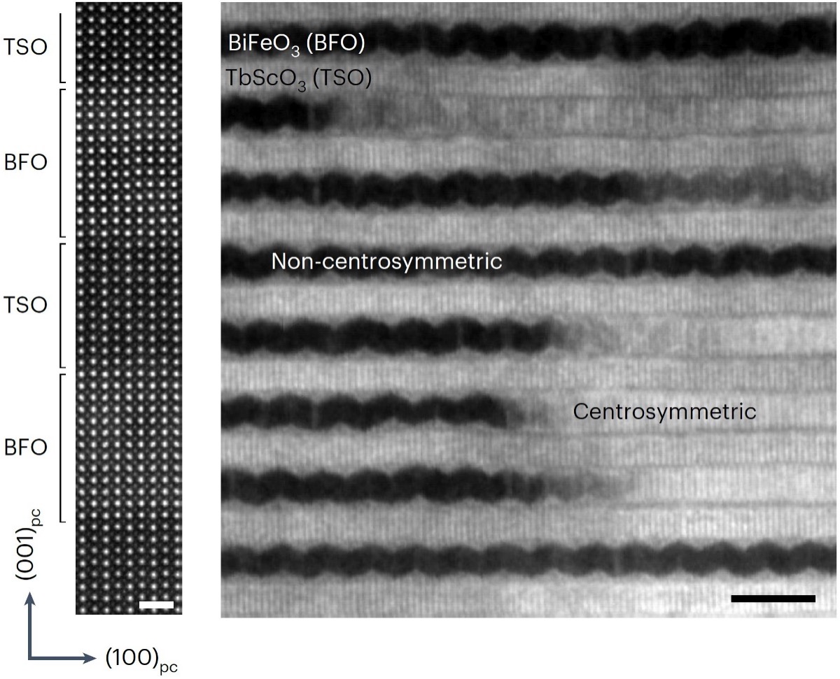
Figure 1: (Left) Atomically resolved High-angle annular dark field STEM image of the [(BFO)14/(TSO)10]20 superlattice along the [010]pc zone-axis showing atomically sharp interfaces (scale bar, 10 nm). (Right) Bright-field image from the scanning convergent beam electron diffraction (SCBED) dataset showing the spatial distribution of polar (Pc) and antipolar (Pnma) BFO phases (scale bar, 10 nm).
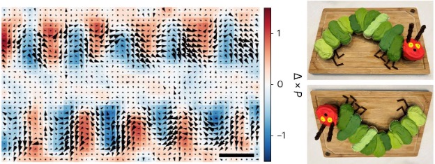
Figure 2: (Left) Polarization map of the polar phase overlaid with its curl (∇×P) obtained by analyzing the Kikuchi bands recorded in the SCBED dataset using an EMPAD. Scale bar, 5 nm. (Right) Caterpillar cake in various shades of green representing the continuously winding electric dipoles in the polarization maps.
The new material is a superlattice of alternating 14-unit-cell-thick BiFeO3 layers and 10-unit-cell-thick TbScO3 layers on a GdScO3 substrate in which a coexistence of centrosymmetric and non-centrosymmetric BiFeO3 phases is stabilized at room temperature with antipolar, insulating and polar, semiconducting behavior, respectively. Both phases are identified and characterized using a combination of high-resolution and four-dimensional (4D) scanning transmission electron microscopy (STEM) at PARADIM, piezoforce microscopy (PFM), and confocal second harmonic generation (SHG) over atomic and mesoscopic length scales.
Crystal symmetry in condensed-matter materials largely dictates their micro- and macroscopic properties, and new material functionalities can arise when inversion symmetry is broken and when symmetry changes. Thus, the ability to control crystal inversion symmetry on demand is of both fundamental and technological importance. Perhaps the most pervasive example of the manifestation of broken inversion symmetry is in ferroelectrics, where crystal structures that inherently break inversion symmetry directly lead to a switchable spontaneous electrical polarization. Recently, the ability to synthesize heteroepitaxial ferroelectric superlattice systems has enabled new methods to control ferroic order and even crystal symmetry. Here, by using BiFeO3/TbScO3 superlattices as our model system, we take advantage of (i) the discontinuity of the spontaneous polarization; (ii) the lattice mismatch; and (iii) the octahedral tilt frustration between the two layers to engineer crystal inversion symmetry. We stabilize both a non-centrosymmetric polar and a centrosymmetric antipolar phase mediated by a first order phase transition at room temperature. Both phases are identified and characterized using a combination of high-resolution and four-dimensional (4D) scanning transmission electron microscopy (STEM), piezoforce microscopy (PFM), and confocal second harmonic generation (SHG) over atomic and mesoscopic length scales. Moreover, applying orthogonal in-plane electric fields to this mixed-phase system results in the deterministic, nonvolatile interconversion of the centrosymmetric and non-centrosymmetric phases, resulting in a three order of magnitude change in the non-linear optical (SHG) response of the system. Demonstration of such an optically addressable, multi-state memory device presents new avenues for cross-functional devices which take advantage of the interconversion between ferro- and anti-ferroelectric states.
Competition between ground states at phase boundaries can lead to significant changes in properties under stimuli, particularly when these ground states have different crystal symmetries. A key challenge is to stabilize and control the coexistence of symmetry-distinct phases. Using BiFeO3 layers confined between layers of dielectric TbScO3 as a model system, we stabilize the mixed-phase coexistence of centrosymmetric and non-centrosymmetric BiFeO3 phases at room temperature with antipolar, insulating and polar semiconducting behavior, respectively. Application of orthogonal in-plane electric (polar) fields results in reversible non-volatile interconversion between the two phases, hence removing and introducing centrosymmetry. Counterintuitively, we find that an electric field ‘erases’ polarization, resulting from the anisotropy in octahedral tilts introduced by the interweaving TbScO3 layers. Consequently, this interconversion between centrosymmetric and non-centrosymmetric phases generates changes in the non-linear optical response of over three orders of magnitude, resistivity of over five orders of magnitude and control of microscopic polar order. Our work establishes a platform for cross-functional devices that take advantage of changes in optical, electrical and ferroic responses, and demonstrates octahedral tilts as an important order parameter in materials interface design.
Accurately mapping polarization in ferroelectric layers by transmission electron microscopy can be challenging. Slight variations in sample tilt dramatically affect the resulting polarization map. Such tilts are commonly in ferroelectrics due to disclination strain. For this superlattice, the microstructure of the BiFeO3 grains at first resembles 109° domain walls. Were this the case, the curl of the polarization (what is plotted in color in the figure) would be zero inside of each domain and only non-zero in the vicinity of the domain wall. The microscopy experts in PARADIM’s Electron Microscopy Facility developed a very accurate polarization mapping technique that is used in this work. It uses Kikuchi bands in the convergent beam electron diffraction pattern collected at each point by PARADIM’s second-generation electron microscopy pixel array detector to avoid small sample tilts and achieve an accurate polarization map. As can be seen in the figure, the curl of the polarization is non-zero in most of the BiFeO3 portion of the superlattice. These are not simply 109° domains, but instead a new phase of BiFeO3 that is non-centrosymmetric and shows continuously winding electric dipoles resembling a polarization wave or a series of half-vortices
L. Caretta, Y.-T. Shao, J. Yu, A.B. Mei, B.F. Grosso, C. Dai, P. Behera, D. Lee, M. McCarter, E. Parsonnet, Harikrishnan K.P., F. Xue, X. Guo, E.S. Barnard, S. Ganschow, Z. Hong, A. Raja, L.W. Martin, L.-Q. Chen, M. Fiebig, K. Lai, N.A. Spaldin, D.A. Muller, D.G. Schlom, and R. Ramesh, "Non-Volatile Electric-Field Control of Inversion Symmetry," Nat. Mater. 22, 207–215 (2023). DOI: 10.1038/s41563-022-01412-0.
R.R., L.W.M., D.A.M., L.-Q.C. and D.G.S. acknowledge support from the Army Research Office under the ETHOS MURI via cooperative agreement W911NF-21-2-0162. The MIM work (J.Y., D.L. and K.L.) was supported by the Office of Science, Office of Basic Energy Sciences, of the US Department of Energy under contract no. DE-SC0019025. Computational resources were provided by ETH Zürich and the Swiss National Supercomputing Center (CSCS), project ID no. s889. Work at ETH was supported by ETH Zürich and the Körber Foundation. M.F. acknowledges support by the Swiss National Science Foundation project 200021_178825. Z.H. and X.G. were supported by the National Natural Science Foundation of China grant no. 92166104. Work at the Molecular Foundry was supported by the Office of Science, Office of Basic Energy Sciences, of the US Department of Energy under contract no. DE-AC02-05CH11231. L.C. acknowledges financial support from the Ford Foundation and the University of California President’s Postdoctoral Fellowship Program. Y.-T.S. and D.A.M. acknowledge financial support from the Department of Defense, Air Force Office of Scientific Research under award FA9550-18-1-0480. The electron microscopy studies were performed at the Cornell Center for Materials Research, a National Science Foundation (NSF) Materials Research Science and Engineering Centers program (DMR-1719875, NSF-MRI-1429155). The microscopy work at Cornell was supported by the NSF PARADIM (DMR-2039380), with additional support from Cornell University, the Weill Institute and the Kavli Institute at Cornell. The authors acknowledge discussions regarding diffraction imaging with J.-M. Zuo as well as M. Thomas, J.G. Grazul, M. Silvestry Ramos and K. Spoth for technical support and careful maintenance of the instruments. We thank X. Huang, A. Fernandez and P. Meisenheimer for fruitful conversations and M.E. Holtz for preliminary electron microscopy studies. We also acknowledge I. Schulze-Jonack and M.S. Stypa for help with substrate crystal growth.