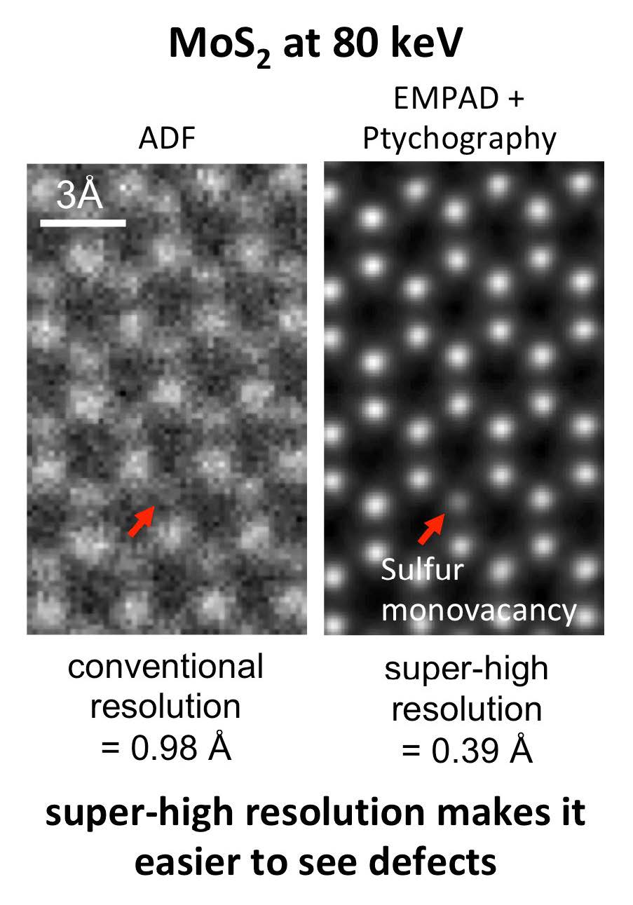
Electron microscopy is a widespread and often essential tool for structural and chemical analysis at the atomic level. Image resolution is dominated by the energy (or wavelength) of the electron beam and the quality of the lens. Two-dimensional valleytronic materials are imaged with low beam energies to avoid damaging the samples, limiting spatial resolution to ~1 Å. By combining our new design of electron microscope pixel array detector (EMPAD) which has the dynamic range to record the complete distribution of transmitted electrons at every beam position, and a phase retrieval algorithm to process the data, PARADIM’s in-house research team has increased the spatial resolution well beyond the traditional lens limitations, reaching a new world record for spatial resolution. As is apparent in the image on the right taken at a beam energy of 80 keV, the ptychographic reconstructions significantly improve the image contrast of single- atom defects in MoS2, corresponding to a 0.39 Å Abbe resolution, at the same dose and imaging conditions where conventional imaging modes reach only 0.98 Å. This new super-resolution imaging is available to PARADIM users utilizing the new EMPAD detector in combination with ptychography available in (and only in) PARADIM’s electron microscopy user facility.
|
| Figure: Two TEM images of MoS2 measured at 80keV. Left: In conventional dark field the individual atoms are barely visible. Right: The super high resolution of the EMPAD detector and ptychography makes it easer to see defects (single sulfur vacancy) among well-resolved individual atoms |
Reference: Y. Jiang et al. Nature 559 (2018) 343–349.
Technical details:
It has long been recognized that the information limit set by diffractive optics is not an ultimate limit. Instead, there is phase information encoded throughout a diffraction pattern formed from a localized electron beam. It is in the form of interference patterns between overlapping scattered beams, and as the incident localized beam is scanned, the phase information and hence the interference patterns change in a predictable manner that can be used to retrieve the phase differences, an approach known as ptychography. While originally conceived to solve the phase problem in crystallography, ptychography has received renewed attention as a dose-efficient technique to recover the projected potential of materials, with modifications to measure finite thickness and three-dimensional samples. In principle. the resolution is limited by the largest scattering angle at which meaningful information can still be recorded, however, as electron scattering form factors have a very strong angular dependence, the signal falls rapidly with scattering angle, requiring a detector with high dynamic range and sensitivity to exploit this information.
To date, ptychography has been widely adopted for light and x-ray applications, yet the technique is still under-explored in transmission electron microscopy in large part because of the detector challenges. Traditional electron cameras such as charge-coupled devices (CCDs) and pixelated detectors have been hampered by slow readout speeds or poor dynamic ranges. Previous work has mainly made use of electrons only within the bright field disk and thus image resolution did not overcome the 2α limit imposed by the physical aperture. We developed and employ a new type of electron microscope pixel array detector (EMPAD) that is capable of recording all the transmitted electrons with sufficient sensitivity and speed to provide a complete ptychographic reconstruction. Our EMPAD design has a high dynamic range of 1,000,000:1 while preserving single electron sensitivity with a signal-to-noise ratio of 140 for a single electron at 200 keV. The detector retains a good performance from 20-300 keV. Here we operated at 80 keV where the noise per pixel is 1/50 of an electron, the detective quantum efficiency is 0.96, and the maximum beam current per pixel is 5 pA. By utilizing essentially all collected electrons (99.95% of the incident beam), with a full 4D data set acquired in typically a minute, our full-field ptychographic reconstructions more than doubles the image resolution compared to the highest-resolution conventional imaging modes such as annular dark field STEM.
The work was recognized as the highest resolution microscope (of any type) by Guinness World Records in July 2018.
Full Reference: Y. Jiang, Z. Chen, Y. Han, P. Deb, H. Gao, S. Xie, P. Purohit, M. W. Tate, J. Park, S. M. Gruner, V. Elser, and D. A. Muller. “Electron Ptychography of 2D Materials to Deep Sub-Ångström Resolution,” Nature 559 (2018) 343–349.
Return to: In-house Research Highlights