PARADIM Highlight #120—In-House Research (2026)
David A. Muller (Cornell)
Next-generation semiconductor devices are adopting feature sizes of just a few nanometers, with individual components about a dozen atoms wide. The characterization of such tiny structures for fault-finding and debugging in new computer chips, fuels the need for an adequate atomic-scale metrology.
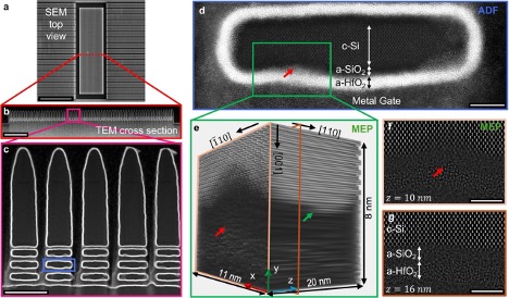
Figure 1: a) Overview SEM image of a gate-all-around test structure node (top view, early process development, expected to contain many defects, scale bar: 3 μm). b) Cross-section (lamella) along red-dotted line showing 63 gate-all-around columns (3 per stack; scale bar: 0.5 μm). c) magnified view, highlighting five columns (scale bar: 50 nm). d) common TEM image of a single structure with labels. The hafnium oxide intrusions into the silicon channel are visible (red arrow, scale bar: 5 nm). e-g) 3D ptychography reconstruction and slices at two depths show interface roughness, hafnium oxide intrusion (red arrow) and a step edge at the crystalline-silicon/amorphous-silicon oxide interface (green arrow); f,g scale bars: 3 nm.
Here, members of the PARADIM In-House Team used our Cornell-designed electron microscope pixel array detector (EMPAD-G2) to collect and reconstruct a three-dimensional view inside a modern device using electron ptychography—a technique that holds the world record in microscopy resolution and is available to all users. In collaboration with semiconductor industry partners a special variety of ptychography is used to calculate a three-dimensional reconstruction of the sample that shows atomic-scale details of buried structures along the narrow silicon channel (d), like hafnium oxide intrusions (red arrows) or step edges (green arrow)—all contributing to interface roughness that can impede the performance of the entire electronic device—features that are either inaccessible or easily missed with conventional imaging methods.
Next-generation semiconductor devices are adopting three-dimensional (3D) architectures with feature sizes in the few-nanometer regime, creating a need for atomic-scale metrology to identify and resolve performance-limiting fabrication challenges. X-ray methods provide 3D information but lack atomic resolution, while conventional electron microscopy offers limited depth sensitivity. The PARADIM Team demonstrates how multislice electron ptychography, a computational microscopy technique with sub-Ångström lateral and nanometer-scale depth resolution, enables 3D imaging of buried device structures. The technique is used to image a prototype gate-all-around transistors and directly quantify roughness, strain, and defects at the interface of the 3D gate oxide wrapped around the silicon channel. The silicon in the 5-nm-thick channel relaxes away from the interfaces, leaving only ~60% of atoms in a bulk-like structure. From a single dataset, ptychography provides quantitative metrology of atomic scale interface roughness in 3D, previously accessible only through indirect inference, along with strain and other structural parameters needed for device modeling and process development.
The fabrication of modern electronic devices takes hundreds, if not thousands, of steps of chemical etching, deposition, and heating, and along the way every single step impacts the final structure. State of the art uses projective images to try to understand what was really going on. Now, the new approach developed by the PARADIM team provides a direct probe to analyze the structures after every single step and have a better grasp of every individual processing step. The new imaging capability could potentially impact almost anything with a modern computer chip, from cellphones to laptops and data centers, and could be a boon for debugging next-generation technologies such as quantum computers, which require extraordinary structural control of materials that is still not fully understood.
The electron microscopy pixel array detector (EMPAD) was developed at Cornell University and in-part supported by PARADIM. The reconstruction via multislice electron ptychography was developed by the PARADIM In-House Research Team.
S. Karapetyan, S.E. Zeltmann, G. Wilk, T.-K. Chen, V.D.-H. Hou, and D.A. Muller, "3D Atomic-Scale Metrology of Strain Relaxation and Roughness in Gate-All-Around (GAA) Transistors via Electron Ptychography," Nat. Commun. 17, 3561 (2026), DOI: 10.1038/s41467-026-69733-1
S.K., D.A.M. acknowledge funding from TSMC through a Joint Development Project (JDP184087). S.E.Z. acknowledges funding from the Platform for the Accelerated Realization, Analysis, and Discovery of Interface Materials (PARADIM), which is supported by the National Science Foundation under Cooperative Agreement No. DMR-2039380. This work made use of the electron microscopy facility of PARADIM and Cornell Center for Materials Research shared instrumentation facility with Helios FIB supported by NSF (DMR-1539918). The authors also thank Malcolm Thomas, Mariena Silvestry Ramos, Philip Carubia, and John Grazul for technical support and maintenance of the electron microscopy facilities. The authors gratefully acknowledge Michael Givens (ASM), Naoto Horiguchi (imec), Hans Mertens (imec), and Hiroaki Arimura (imec) for providing the Gate-All-Around (GAA) sample used in this study. We thank Jiangtao Zhu and Eurofins Nanolab Technologies for preparing the GAA TEM lamella used in this study. We thank Frieder Baumann for the c-Si/a-SiO2 structural model, Richard Aveyard and Bernd Rieger for the pMOS structural model. S.K. gratefully acknowledges Harikrishnan K.P., Ariana Ray, and Salva Rezaie for training and tutorials on MEP, Dasol Yoon for insightful discussions on multislice simulations, Xiyue Zheng for sharing the automated DPC acquisition code, and Yi Jiang for helpful discussions about MEP. S.K. thanks Lopa Bhatt for developing and sharing a tilt propagator extension to the fold-slice code used in this study.
Data Availability:
Datasets and developed software codes are available at DOI: 10.5281/zenodo.15882443.