PARADIM Hightlight #38 -- Local User Research (2021)
D.G. Schlom, G.H. Xing, D. Jena, Cornell University and Z.-K. Liu, Pennsylvania State University
PARADIM’s in-house team worked with a collaborator at Penn State to develop a new variant of MBE that we call “suboxide MBE.” In contrast to conventional MBE where the molecular beams are elemental, in suboxide MBE the molecular beams are pre-oxidized. Achieving the desired suboxide beams relies on extensive thermodynamic calculations made for the entire periodic table, as shown in Figure 1. [1]
Figure 1: Journal cover of APL Materials, Issue August 2020, highlighting K.M. Adkison et al. APL Mater.8, 081110 (2020).
Seeing how well suboxide MBE works, this variant is now being used in 15 user projects! A recent publication from one of these users demonstrates its promise for the growth of the high-mobility, high-bandgap semiconductor βGa2O3.
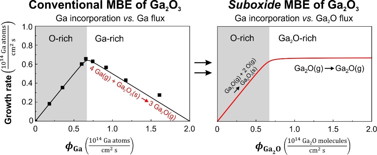
Growing β-Ga2O3 by conventional MBE is quite challenging because it involves a 2-step oxidation reaction to go from the elemental Ga(g) of the molecular beam to Ga2O3(s):
2 Ga + O Ga2O followed by Ga2O + 2 O Ga2O3
This results in a rather complex growth regime.
Using suboxide MBE at PARADIM, the first step is bypassed by supplying a 99.98% pure molecular beam of pre-oxidized Ga2O. The result is a dramatic increase in the growth rate of device-quality b-Ga2O3 films that can readily be made sufficiently thick for vertical devices.
Challenges of conventional MBE:
- Low growth rate (~0.2μm/hr)
- Difficult to control
- Gallium vacancy defects
Advantages of suboxide MBE
- Growth Rate > 1μ/hr
- Smoother surfaces
- Higher Structural surfaces
- Lower growth temperature
This paper employs a newly established growth method—suboxide molecular-beam epitaxy (S-MBE) [1]—which enables a drastic enhancement in the growth rates of Ga2O3 and related materials to over 1 μm h−1 in an adsorption-controlled regime, combined with excellent crystallinity. Using a Ga + Ga2O3 mixture with an oxygen mole fraction of x(O) = 0.4 as an MBE source, kinetic limits are overcome that had previously hampered the adsorption-controlled growth of Ga2O3 by MBE. Here, the user achieved growth rates up to 1.6 μm h−1 and 1.5 μm h−1 for Ga2O3/Al2O3 and Ga2O3/Ga2O3 structures, respectively.
Using S-MBE, allows the growth of phase-pure, smooth, and high-purity homoepitaxial Ga2O3 films that are thicker than 4.5 μm and that exhibit very high crystalline quality at unparalleled low growth temperature. With the enhanced quality and high growth rate of S-MBE, we anticipate a significant improvement to vertical Ga2O3-based devices. We describe and demonstrate how this growth method can be applied to a wide range of oxides. With respect to growth rates and crystalline quality, S-MBE rivals leading synthesis methods currently used for the production of Ga2O3-based devices.
[1] K.M. Adkison, S.-L. Shang, B.J. Bocklund, D. Klimm, D.G. Schlom, and Z.-K. Liu, "Suitability of Binary Oxides for Molecular-Beam Epitaxy Source Materials: A Comprehensive Thermodynamic Analysis," APL Mater.8, 081110 (2020), DOI 10.1063/5.0013159—a PARADIM publication selected as journal cover for APL Materials, Issue August 2020.
Importance of the Achievement: Suboxide MBE is a new variant of MBE that provides advantages for the synthesis of many oxygen-containing compounds. In this paper comprehensive calculations were made for binary oxides of the entire periodic table—128 binary oxides in all—plus an additional 27 two-phase mixtures of binary oxides with their elements. These calculations established the promise of this approach, at least from a thermodynamic perspective. 16 binary oxides were determined to evaporate nearly congruently. Another 24 binary oxides were identified that can provide molecular beams of suboxide species. Note that in contrast to conventional MBE where the molecular beams are elemental, in suboxide MBE the molecular beams are pre-oxidized. Having the species arrive to the growth surface pre-oxidized in the desired oxidation state can be very useful. It provides a means to navigate reaction pathways. By way of example, consider trying to make compounds containing tin in the 2+ oxidation state. Achieving Sn2+ by conventional MBE involves trying to oxidize the incident molecular beam of elemental tin just enough to become Sn2+ and not so much that it becomes Sn4+. To date, this has never been achieved. One either sees tin metal, Sn4+, or a mixture of the two when trying to oxidize tin with an oxidant in MBE growth.
Being able to supply SnO as a pure, pre-oxidized molecular beam has advantages. Indeed, it was exactly this suboxide MBE route that was used by PARADIM user Professor Chang-Beom Eom from the University of Wisconsin-Madison to realize the antiperovskite Sr3SnO (see PARADIM Highlight #28). Controlling oxidation is key to the formation of Sr3SnO and by providing a molecular beam of SnO, the oxidation can be controlled. Another suboxide molecular beam of interest is GeO. It was by providing a molecular beam of GeO that PARADIM user Professor John Heron from the University of Michigan was able to navigate reaction pathways to realize epitaxial films of the rutile polymorph of GeO2 that he desired (see PARADIM Highlight #32). Suboxide MBE has enabled never before synthesized epitaxial films of Sn2+ materials to be realized, BaSnO3 films to be grown with the highest mobility in the world, VO2 films with ultra-sharp metal-insulator-transitions, and additional challenging electronic materials.
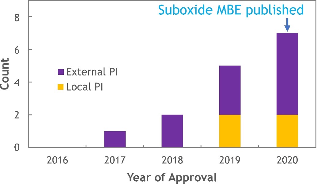 Figure 3: Approved PARADIM proposals utilizing suboxide MBE.
It took PARADIM’s In-House team working with a collaborator of the Platform 3 years to develop the comprehensive thermodynamic understanding underlying suboxide MBE. That itself is not unusual. What is unusual, at least from the traditional means of informing others through publication, is that PARADIM began openly sharing the concept of suboxide MBE and preliminary thermodynamic calculations with its users over 2 years prior to publication. This is part of the brainstorming that occurs among members of the Platform as they formulate plans to attempt to make new materials. This goes beyond just informing users of what has been done, but actively brainstorming as a team how to approach the synthesis of their specific systems of interest to realize what has never before been achieved. The histogram in Figure 3 shows the speed with which suboxide MBE is being used by the broader community in a total of 15 user projects (until end of 2020). Note how quickly external users have become aware of the technique and have been able to apply it to the realization of materials of interest to them. This is a different way of doing business; it demonstrates the power of a MIP.
P. Vogt, F.V.E. Hensling, K. Azizie, C.S. Chang, D. Turner, J. Park, J.P. McCandless, H. Paik, B.J. Bocklund, G. Hoffman, O. Bierwagen, D. Jena, H.G. Xing, S. Mou, D.A. Muller, S.-L. Shang, Z.-K. Liu, and D.G. Schlom, "Adsorption-controlled growth of Ga2O3 by suboxide molecular-beam epitaxy," APL Mater. 9, 031101 (2021); https://doi.org/10.1063/5.0035469.
We thank J. D. Blevins for the Ga2O3(010) substrates from SYNOPTICS used in this study and are grateful for stimulating discussions with R. Droopad, J. P. Maria, and M. Passlack. K.A., C.S.C., J.P.M., D.J., H.G.X., D.A.M., and D.G.S. acknowledge support from the AFOSR/AFRL ACCESS Center of Excellence under Award No. FA9550-18-1-0529. J.P.M. also acknowledges support from the National Science Foundation within a Graduate Research Fellowship under Grant No. DGE-1650441. P.V. acknowledges support from ASCENT, one of six centers in JUMP, a Semiconductor Research Corporation (SRC) program sponsored by DARPA. F.V.E.H. acknowledges support from the Alexander von Humboldt Foundation in the form of a Feodor Lynen fellowship. F.V.E.H. and H.P. acknowledge support from the National Science Foundation (NSF) [Platform for the Accelerated Realization, Analysis and Discovery of Interface Materials (PARADIM)] under Cooperative Agreement No. DMR-1539918. J.P. acknowledges support from the Air Force Office of Scientific Research under Award No. FA9550-20-1-0102. S.-L.S. and Z.-K.L. acknowledge the support of the NSF through Grant No. CMMI-1825538. This work made use of the Cornell Center for Materials Research (CCMR) Shared Facilities, which are supported through the NSF MRSEC Program (Grant No. DMR-1719875). Substrate preparation was performed, in part, at the Cornell NanoScale Facility, a member of the National Nanotechnology Coordinated Infrastructure (NNCI), which is supported by the NSF (Grant No. NNCI-2025233). Work by G.H. and O.B. was performed in the framework of GraFOx, a Leibniz-ScienceCampus partially funded by the Leibniz association. G.H. acknowledges financial support by the Leibniz-Gemeinschaft under Grant No. K74/2017. B.J.B. was supported by a NASA Space Technology Research Fellowship (grant number 80NSSC18K1168) and he acknowledges support and training provided by the Computational Materials Education and Training (CoMET) NSF Research Traineeship (grant number DGE-1449785).
Data: Data related to the growth and structural characterization are available at https://doi.org/10.34863/a2jw-kh18.